The complete guide to PCB pad :types, size, spacing, repair and comparison - IBE Electronics
Soldering is one of the most important processes in PCBA processing. On printed circuit boards, electrical connections to all components are made via PCB pads. The PCB pads are a very critical part of the PCB that determines where components are soldered on the PCB.The size, shape, and position of pads in a PCB directly depend on the manufacturing quality of the board. Today we will take a look at the PCB pad in SMT soldering.
Soldering is one of the most important processes in PCBA processing. On printed circuit boards, electrical connections to all components are made via PCB pad.
PCB Via Size and Pad Size Guidelines, Zach Peterson, Blog

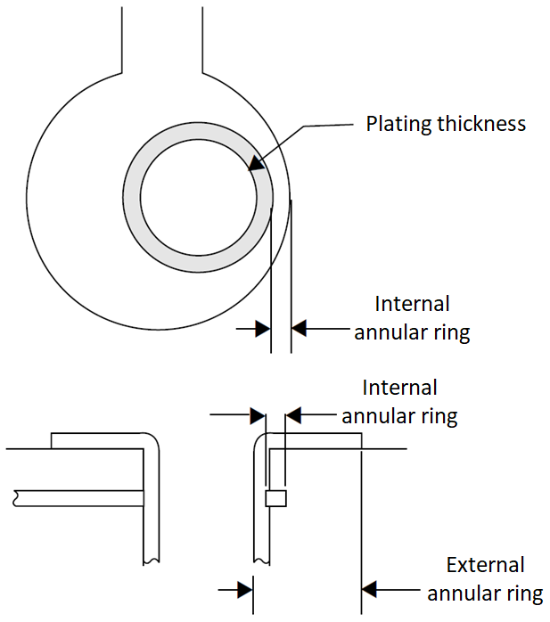
What is Pad to Pad (PP) ?
PCB Layout Design
Ultimate Guide to Cleaning Electronics

Xiaomi Packs 48-megapixel Camera Into Budget Redmi Note, 55% OFF
Small Circuit Board Design: How to Reduce PCB Size
Identifying and Processing Via-In-Pad in PCB Design - JHYPCB

What is a PCB pad - different types and design guidelines - PCBA Manufacturers
The Best Free PCB Design Software of 2023