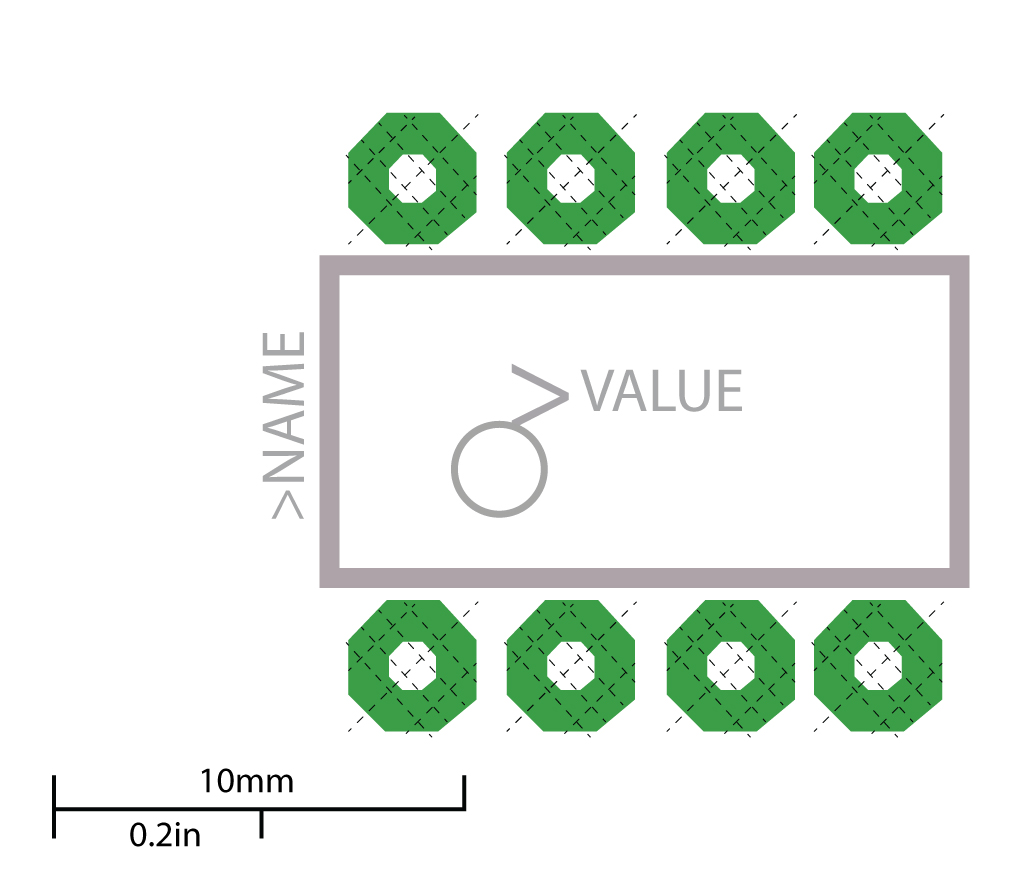
pcb - Connecting pads with the same functionality belonging to one
I have a question about routing style of pads with the same functionality belonging to one chip. I draw a picture in Paint (fictional IC; let it be the SOIC8 footprint). GND is only as example (it
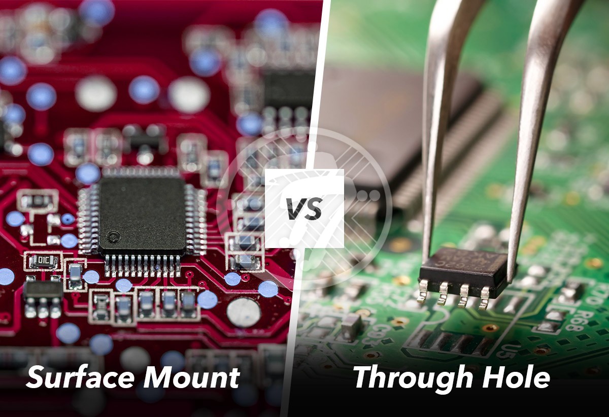
Surface Mount vs Through Hole – Technotronix
How to Use Do-not-populate (DNP) Components in Your PCB Design, PCB

An ultimate guide to PCB gold fingers - IBE Electronics

PCB Design Basics: A Comprehensive Introduction - Zuken US

What is the difference between PCB and PCBA? - RAYPCB
What is a Pad in PCB Design and Development

What is a PCB pad - different types and design guidelines - PCBA Manufacturers

Via-in-Pad - PCB Prototype the Easy Way - PCBWay

Things to Learn Before You Learn PCB Designing - PCB Design Tutorial - PCBway

Key Components of a PCB: Layers, Traces, and Pads Explained - Viasion PCB

What is a Pad in PCB Design and Development
What are Vias in Pad? Advantages, Limitations, Applications, and Comparison with Conventional Vias