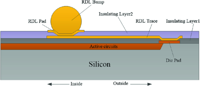
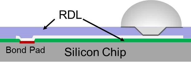
The bond pad redistribution layer (polyimide 1) and the under bump

The bond pad redistribution layer (polyimide 1) and the under bump

Process integration of fine pitch Cu redistribution wiring and SnCu micro-bumping for power efficient LSI devices with high-bandwidth stacked DRAM - ScienceDirect

The bond pad redistribution layer (polyimide 1) and the under bump
NEWS - Strong Electronics&Technology Limited
RDL and Flip Chip Design
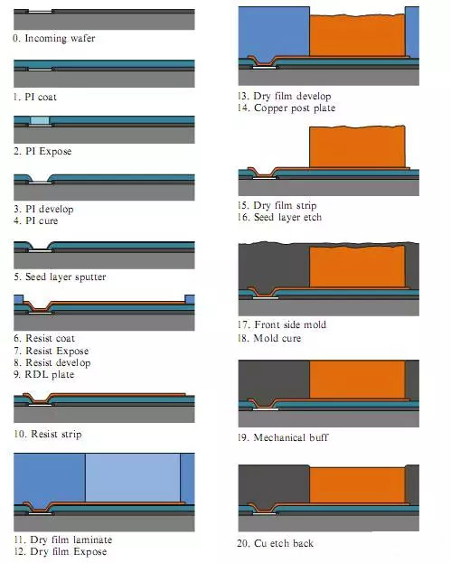
Redistribution Layer (RDL) Technology for ICs Package

Materials, Free Full-Text

Wafer level packaging having bump-on-polymer structure - ScienceDirect
Polymer Challenges in Electronic Packaging: Part 8 Embedded Wafer Level Packaging Materials - Polymer Innovation Blog

US6660624B2 - Method for reducing fluorine induced defects on a bonding pad surface - Google Patents

Redistribution in wafer level chip size packaging technology for high power device applications: Process and design considerations - ScienceDirect

Warren FLACK, Vice President, PhD

Advanced Wire Bonding Technology: Materials, Methods, and Testing

Fan-In Wafer/Panel-Level Chip-Scale Packages
Electromigration Performance Of Fine-Line Cu Redistribution Layer (RDL) For HDFO Packaging