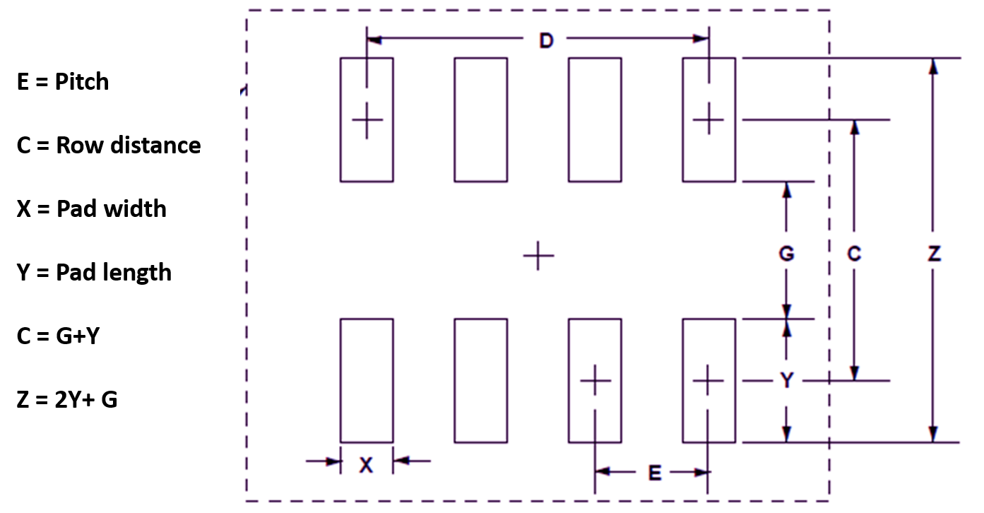
Details of test chip designs: pad pitch, layout, materials, and opening.
4.9
(606)
Write Review
More
$ 12.99
In stock
Description
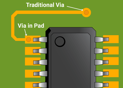
What is a Pad in PCB Design and Development

Semiconductor Back-End Process 5:Package Design and Analysis

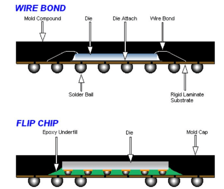
RDL and Flip Chip Design

Integrated circuit - Wikipedia
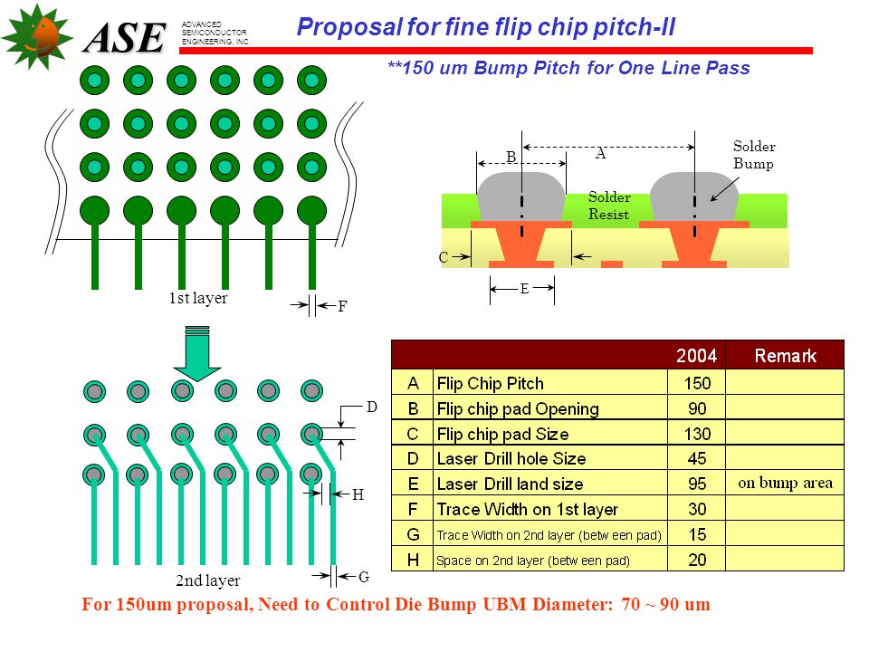
ASE Flip-Chip Build-up Substrate Design Rules - ppt video online download

Shifting Left for Earlier Testing in 2.5D and 3D IC Design
What is a Pad in PCB Design and Development
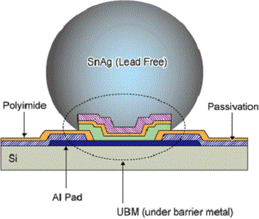
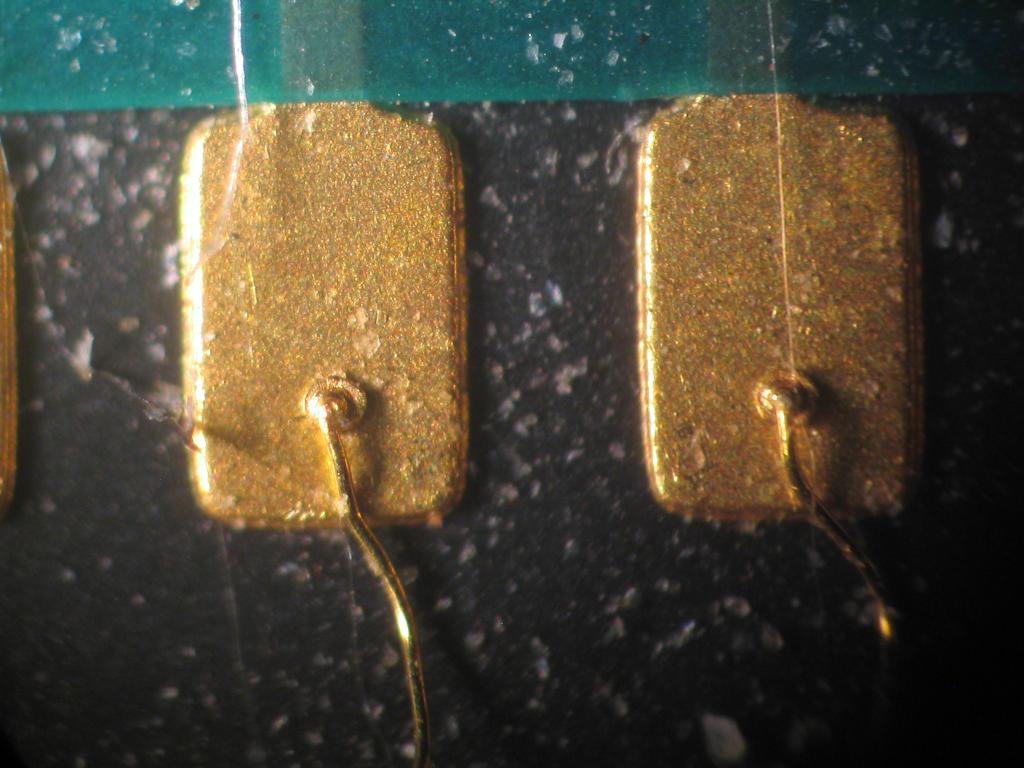
Bump on Pad, Wafer Process Technology

What is a Pad in PCB Design and Development
Top PCB Layout Recommendations for BGA Packages
IC I/O pad layout and choice

FET Test Chips, Optimized for 2D Materials, Platinum
What is a Pad in PCB Design and Development
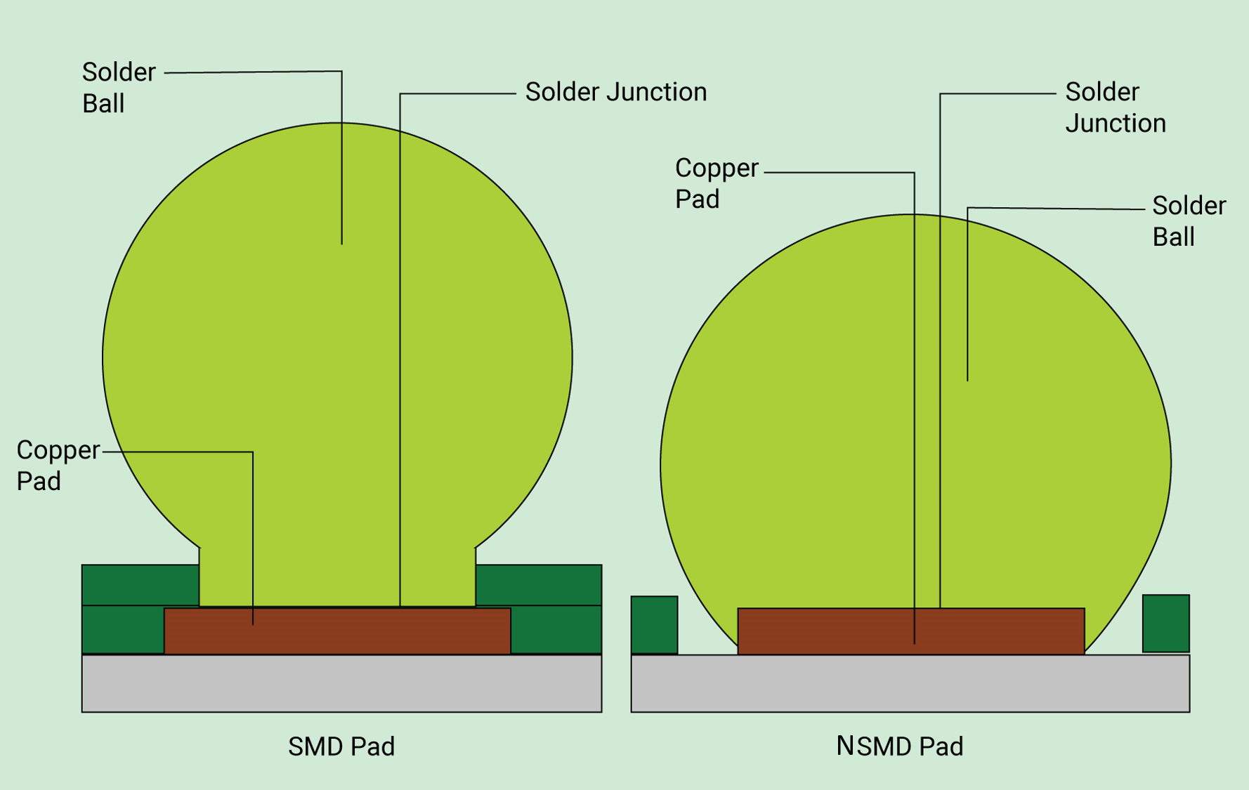
Ball Grid Array Technology Overview
Flip-Chip BGA: PCB Layout Best Practices - Free Online PCB CAD Library
Related products


You may also like