
Figure 2 from Under Bump Metallurgy (UBM)-a technology review for flip chip packaging
Fig. 2. Schematic cross-section of evaporated UBM and solder bump [12] - "Under Bump Metallurgy (UBM)-a technology review for flip chip packaging"
Artificial intelligence deep learning for 3D IC reliability prediction

A study in flip-chip UBM/bump reliability with effects of SnPb
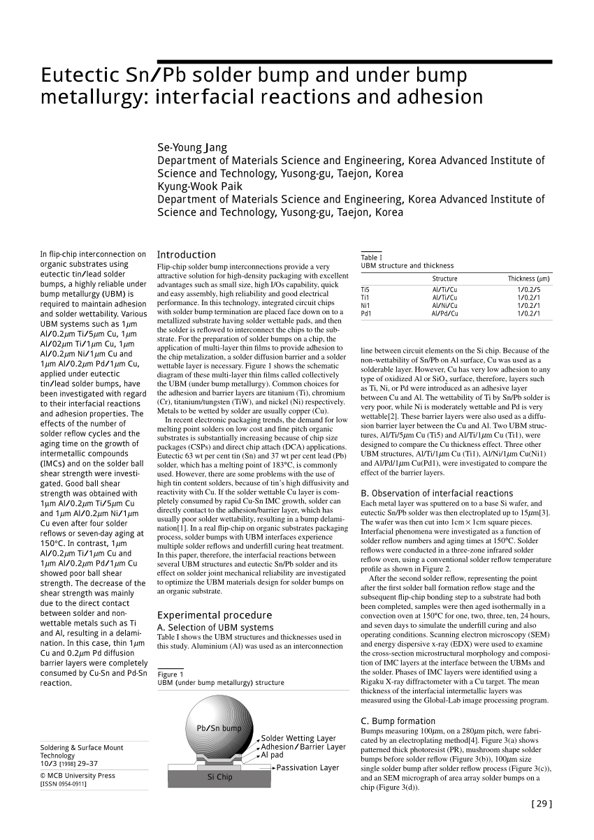
PDF) Eutectic Pb/Sn solder bump and Under Bump Metallurgy
Pb-Free Solders for Flip-Chip Interconnections

Challenges Grow For Creating Smaller Bumps For Flip Chips

C4NP Bumping Process Flow Download Scientific Diagram

A study in flip-chip UBM/bump reliability with effects of SnPb
UBM (OPM: Over Pad Metal, FSM: Front Side Metal and Electroless

Challenges Grow For Creating Smaller Bumps For Flip Chips

Manufacturing processes for fabrication of flip-chip micro-bumps

PDF) Under Bump Metallurgy (UBM)-a technology review for flip chip
Micromachines, Free Full-Text

Figure 2 from Bump formation for flip chip and CSP by solder paste
Challenges Grow For Creating Smaller Bumps For Flip Chips
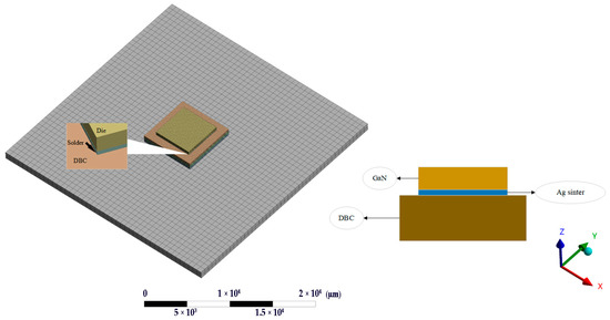
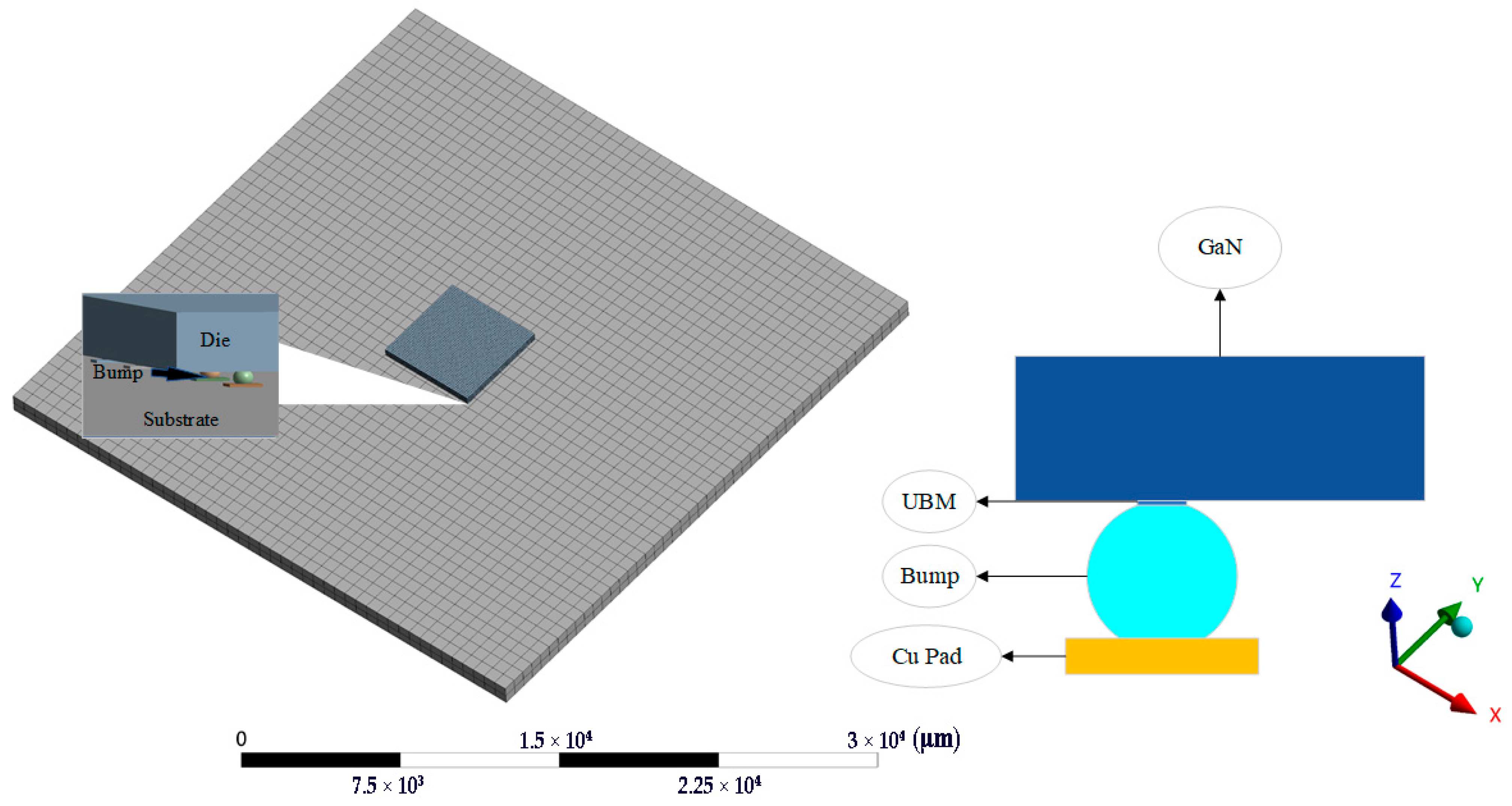
Reliability Analysis of Flip-Chip Packaging GaN Chip with Nano


:max_bytes(150000):strip_icc()/PEO-Down--Feather-Co-Natural-Nights-750-Fill-Power-Goose-Down-Pillows-Light-Yellow-Kaya-Abrahamson-Photo-22-55ef807069b84c2886551e94e37543c7.jpg)
